Case studies

An article by Toshihiko Ogura of AIST (National Institute of Advanced Industrial Science and Technology, Japan) explains the development of “a new type of impedance microscopy, namely multi-frequency impedance SEM (IP-SEM), which allows nanoscale imaging of various specimens in water while minimising radiation damage”.
The research explains the advantages of the method as opposed to standard Scanning Electron Microscopy (SEM) including the ability to “detect dielectric properties of the sample’s composition at nanometre resolution”, to examine “unstained biological specimens and material samples in water” and finally for use with “diverse samples in liquids across a broad range of scientific subjects such as nanoparticles, nanotubes and organic and catalytic materials.”
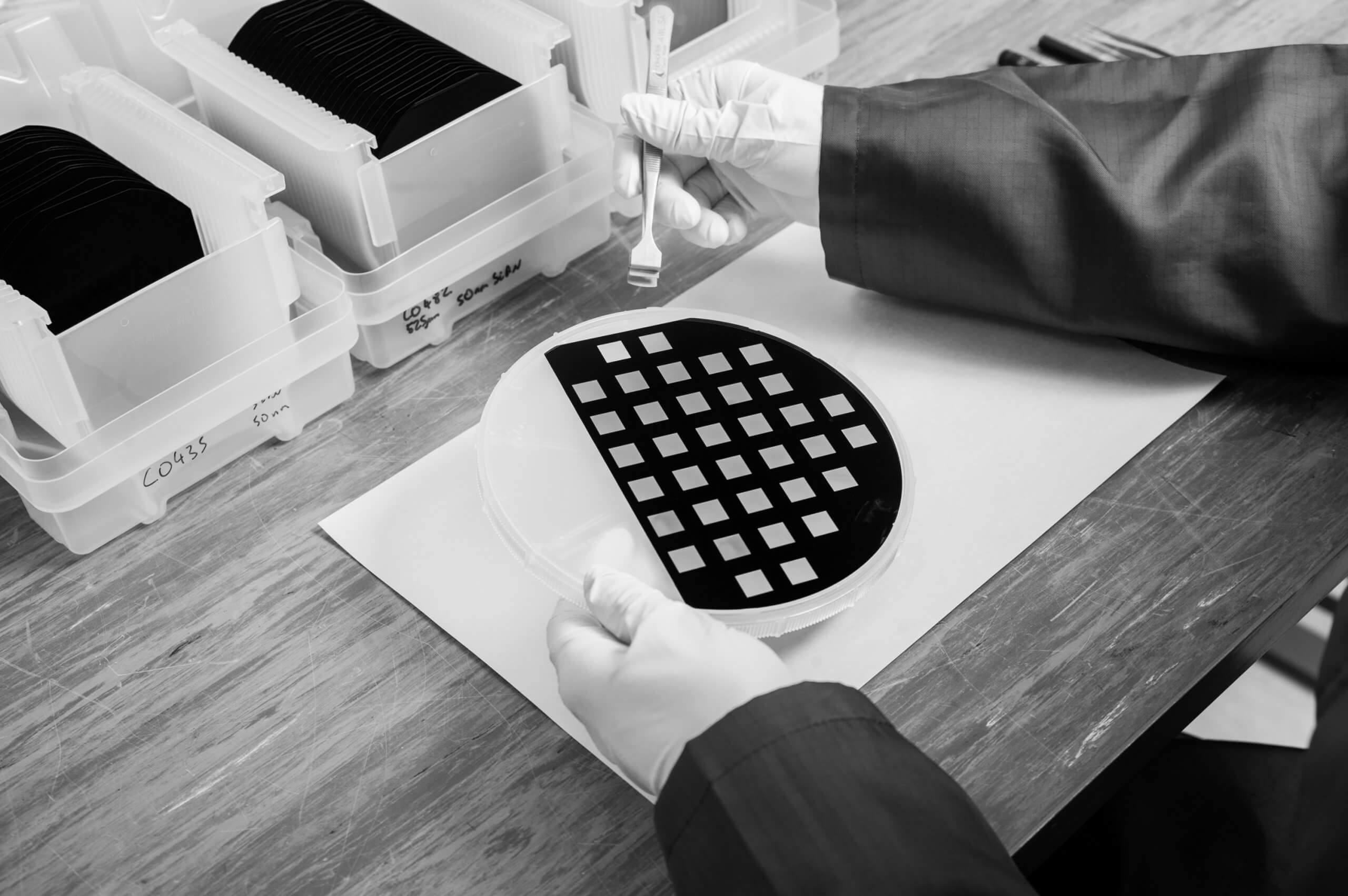
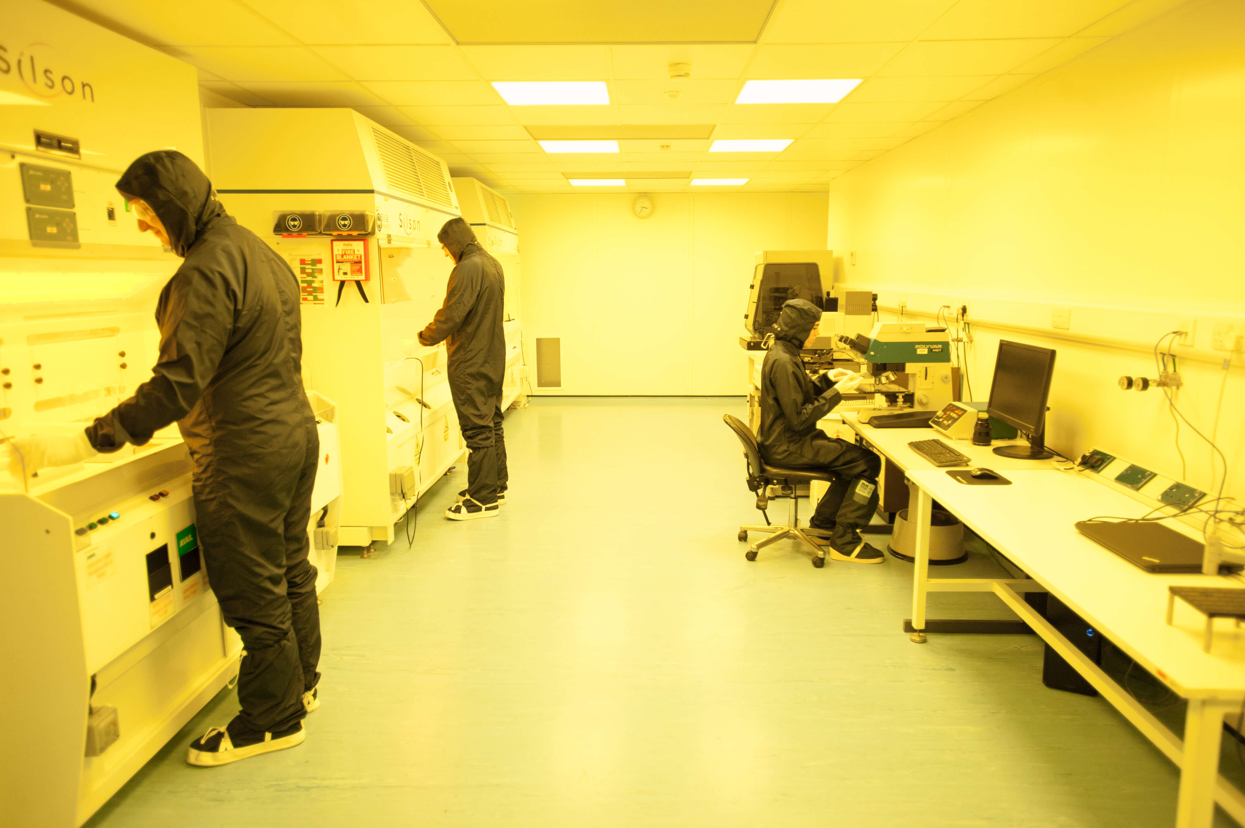
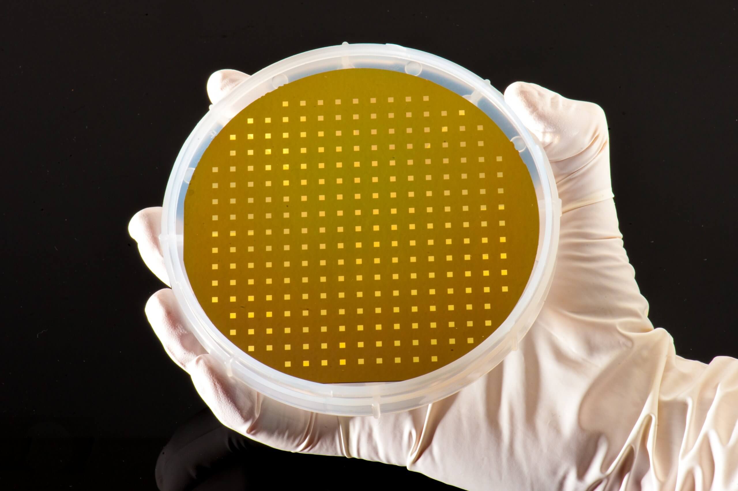
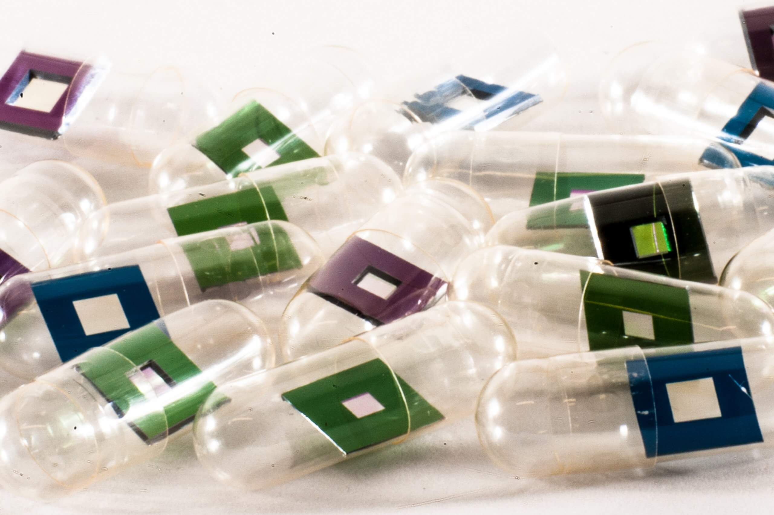
One of Silson’s 50nm thick films was used for the sample preparation procedure, with a frame area of 4.5×4.5 mm2, a membrane area of 0.4×0.4mm2 , and a frame thickness of 0.381 mm.
Follow this link to read more about multi-frequency impedance SEM !