Graphene
We provide our silicon nitride membranes coated with exceptional high-quality mono-layer graphene. Chemical Vapour Deposition is used to grow a single layer of graphene on Copper foil which then is transferred onto a wide range of substrates. Silson’s expertise and capabilities allow us to transfer a high quality film following a very strict wet transfer process developed and improved over the last years.
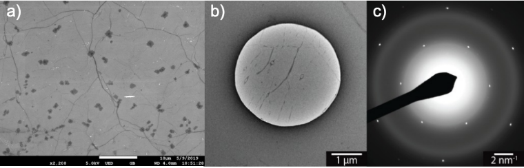
b) TEM image showing a single 3μm coated hole,
c) hexagonal diffraction pattern
For wide ranges of nanomaterials, analysis in the TEM requires that they are deposited on a support material which has an influence in the structural and compositional information that can be obtained. Traditionally thin amorphous carbon films have been used, but graphene offers unique advantages as a TEM support material: it is extremely strong and electrically conductive (to avoid charging under the electron beam), thermally and chemically stable, offers the lowest background contrast possible and provides an inbuilt calibration for both
imaging and diffraction.
Using graphene-based supports has enabled high resolution imaging and analysis of nanoparticles, polymeric assemblies, virus and DNA samples by cryo-EM, and even the atomic resolution observation of the rotation of a single molecule.
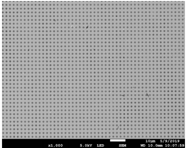
graphene on 1.2μm hole array
monolayer graphene
Graphene specifications
• Appearance (colour): Transparent
• No of graphene layers: 1 (monolayer)
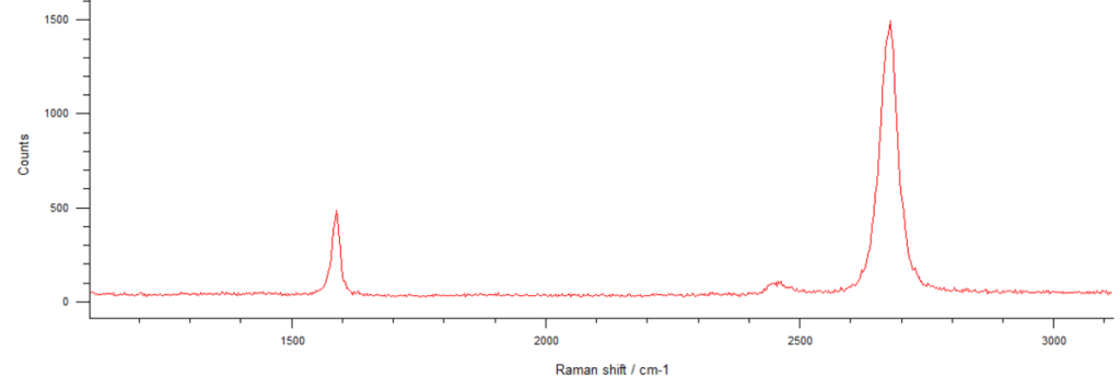
• Raman D/G ratio: 0.05
• Grain size: Up to 100 μm
• Coverage in perforated membranes:
>95% for 1-1.2μm holes
>80% for 2μm holes
Substrate options
Substrates can be chosen between perforated or standard membranes with the option of metals coating. Other product customizations are available on request.
- Standard silicon nitride membranes as individual frames
- Windows for TEM
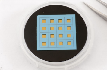
- Multi frame arrays, including TEM MFAs:
1. MFA1: 23.5 x 23.5 mm2 with different arrays
2. MFA2: 17.5 x 17.5 mm2 with different arrays
3. MFA3: 14 x 14 mm2 with different arrays - Perforated silicon nitride membranes:
arrays from 1 μm holes & 2μm pitch to 5 μm holes & 10 pitch

*Other substrates and sizes are available on request, including larger apertures.