Silicon
Mono-crystalline (100) Silicon Membranes
Thin silicon membranes are an excellent alternative to silicon nitride when the presence of nitrogen is detrimental to the application, and also offer higher transmission in the soft x-ray / extreme ultraviolet (EUV) region. The silicon used to form these membranes is conductive, which is advantageous for applications where a conductive sample support is required, for example to minimise charging effects in electron microscopy. Also, as a single crystal (100) substrate, the membranes are ideal for epitaxial growth of a wide range of materials.
Membranes are available in (100) silicon with thicknesses of 50, 75, 100, 150, 200, 2,000, 5,000, 7,000 and 10,000 nm.
Standard frame sizes for silicon membranes are TEM, 5.0, 7.5, 10.0, 12.5, 14.0, 17.5 and 23.5 mm. Standard membrane sizes vary from 20.0 microns to 19.0 mm but Silson can rapidly respond to requests for custom designs.
In addition to the standard square membranes in square frames, rectangular frames and membranes are produced and also windows consisting of multiple membranes on single frame, either for experimental compartmentalisation or to increase the stability of large area membranes.
Membranes with thickness 200nm and thinner are available with silicon frame thickness 200 µm and membranes with thickness 2000nm and thicker are available with silicon frame thickness 300 µm. The standard frame option is prime grade, boron-doped (p type) silicon with resistivity from 1 – 30 ohm-cm with a surface roughness of less than 0.5nm
Every membrane is inspected for ultimate quality assurance and packaged in individual capsules for the best protection during transportation.
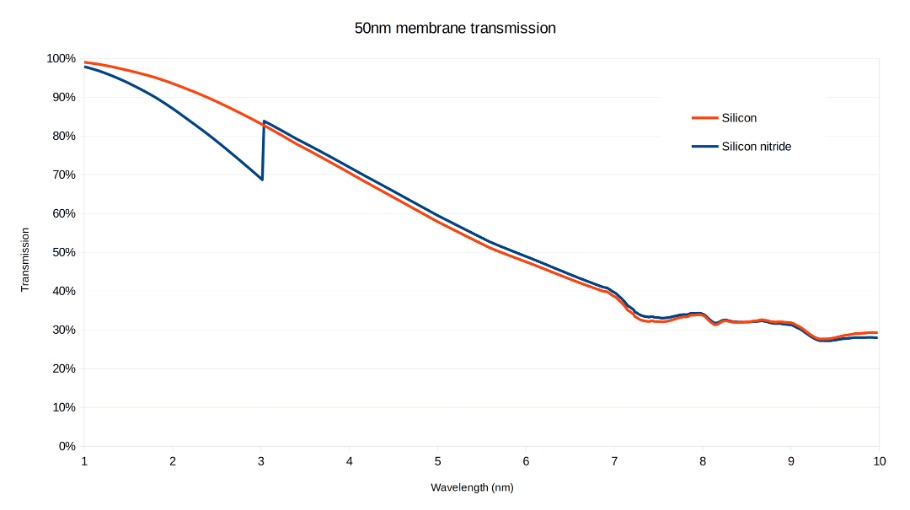
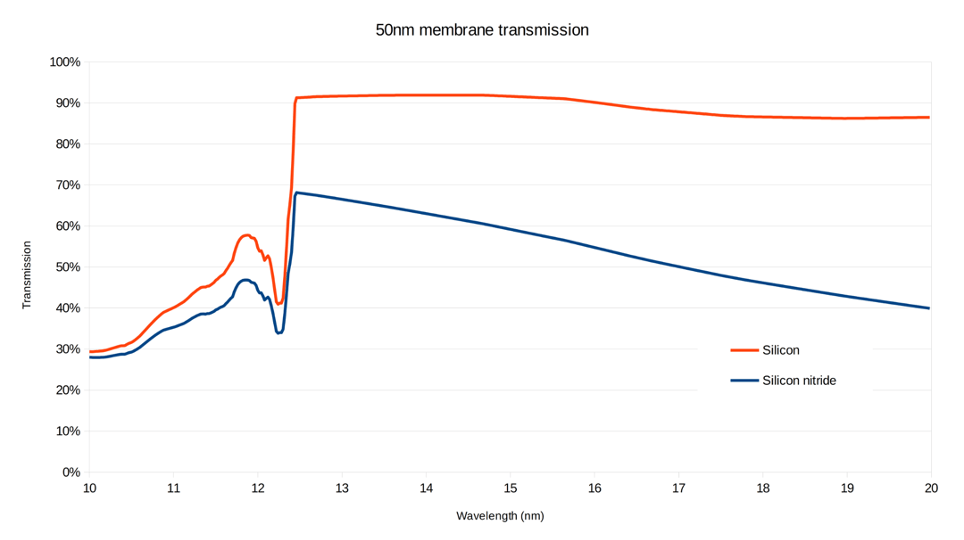
Simulated soft x-ray transmission of a 50nm thick silicon membrane, with comparison to silicon nitride. (Data source: LBL CXRO X-ray database)
Silson recommends the CXRO database for calculations of the transmission of their thin membranes. You can find this page here.
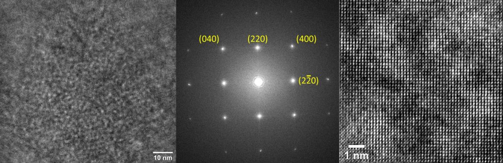
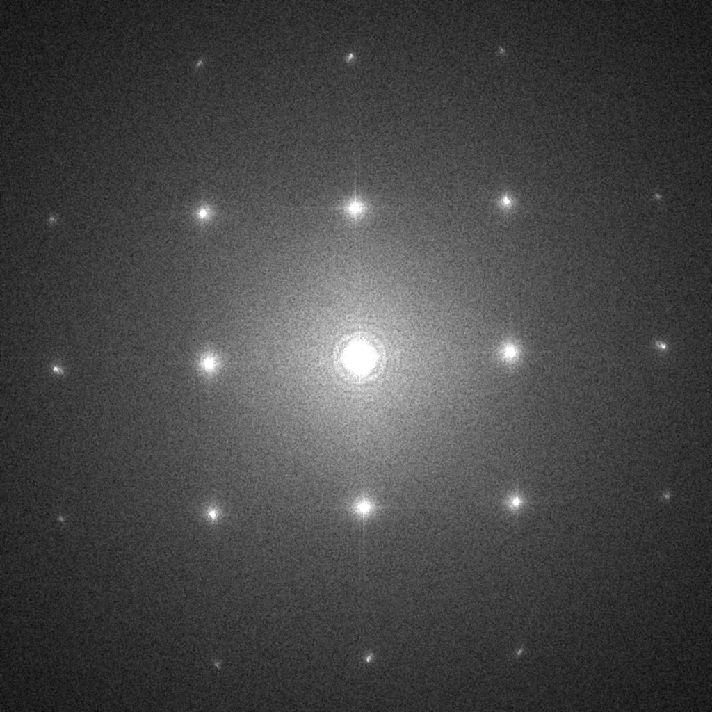
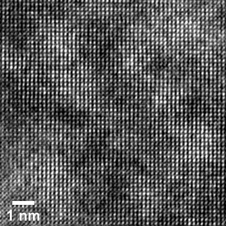
The images below show the crystallinity of the (100) silicon membrane – Courtesy of Mateus G. Masteghin from Advanced Technology Institute – University of Surrey