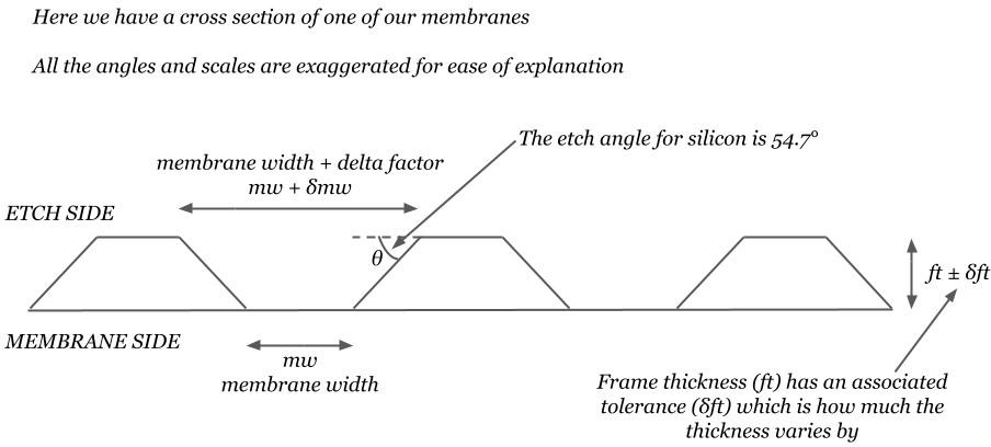
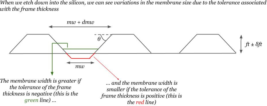
Silicon Etching
Silson’s standard fabrication procedure for producing membranes on silicon substrates uses anisotropic etching. In this process, the (100) direction of the silicon crystal lattice etches at more than 100 times the rate of the (111) direction. Because the membrane films are grown on (100) orientation wafers, these substrates etch down at an angle of 54.7°, which is the angle between the (100) and (111) crystal planes in the silicon face-centered cubic (FCC) lattice.
This etch angle means that to produce a specific membrane size, a slightly larger opening must be defined on the back surface of the wafer which then reduces during the etching process. We refer to this as the delta (𝛿) factor; the mask used to produce the required membranes is defined to account for this delta factor. Silicon wafers are supplied with varying thicknesses within a known tolerance and so the final membrane size will vary according to this tolerance. Typical wafer thickness tolerance is approximately +/- 10μm but there is also a similar total thickness variation (ttv) across an individual wafer. These thickness variations produce membrane size variations of almost exactly the same size so membranes produced with the same mask on wafers of the same nominal thickness may vary in size by 20μm or slightly more.
For most membranes, this size variation is imperceptible but for very small membranes, typically 50μm or smaller, it is significant and so the tolerance on small membranes as a percentage is very high.
Take a look at the diagrams below for an illustration of the silicon etching: